Micro-nano foundry-packaging process reference
Newstime: 2020-07-10 17:49:54
Packaging in micro-nano foundry is the most critical and expensive step. Many semiconductor companies have their own research and opinions on packaging. In foreign countries, STMicroelectronics uses a low-cost packaging method, which is one of the characteristics of its production of inertial sensors. At the same time, through mass production, lower costs can be obtained.
The packaging method they adopted is: use a glass powder low-temperature wafer-level bonding process to enclose the inertial sensor in a closed cavity between the two wafers, and then use a grid array (LGA) packaging platform technology to package chip. In this process, parallel structure and stacked packaging are used. This method can be used for reference in micro-nano foundry packaging.
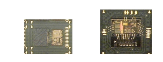
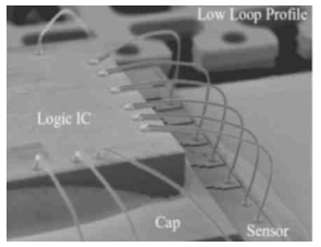
STMicroelectronics uses an adhesive film to solder the sensor die to a substrate with a large surface area in the stacked structure. The stacked placement of semiconductor die and MEMS die can make the package very small. Wire bonding is used to connect the electrical contacts of the two dies, and then the die is packaged using injection molding packaging technology. This packaging method can be completed on a large-area substrate, so the cost is relatively cheap. Packaging stress, especially the stress generated by the bonding and injection molding process, has been a major challenge for this packaging technology. STMicroelectronics successfully solved this problem. The evolution of ST's ultra-compact linear accelerometer package. Linear accelerometers are widely used in consumer electronics.
The packaging step in micro-nano foundry needs to be integrated into the design at all times. The high cost of expenditure makes many companies continue to test and research low-cost packaging methods, the ultimate goal is to obtain profits, while promoting good products to the public. YW MEMS can provide the packaging steps involved in micro-nano foundry, and the process can be designed according to requirements.



 Links:

