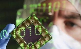
Package design in micro-nano foundry
Newstime: 2020-07-09 17:48:05
Chip packaging is also a part of micro-nano foundry, and many MEMS product vendors will use packaging as a reference for product differentiation and market competition. Moreover, in the design of MEMS devices, packaging methods are all parts of the design process that must be considered. Since packaging costs account for 20%-40% of all costs, this step is even more important. The choice of packaging strategy is slightly important.
The packaging design in micro-nano foundry is slightly more complicated than ordinary packaging, because the craftsman must not only meet the design needs, but also meet the needs in harsh environments. The environment of MEMS devices is very special, such as shock, vibration, dryness, liquid, and humidity.
The packaging of MEMS devices must be able to interact with the environment. For example, the pressure input of the pressure sensor, the fluid inlet of the blood processing device, etc. The packaging of MEMS devices must also meet other mechanical and heat dissipation margin requirements. As the output of the MEMS device, it may be the change of the mechanical motor or the pressure. Therefore, the mechanical parasitics of the package may interact and interfere with the function of the device.
MEMS devices designed in the micro-nano foundry sometimes also use wafer-level packaging, while the protective cap seals the MEMS to achieve isolation from the external environment or to provide mobile protection for the MEMS device before the next packaging. This technology is often used in the packaging of inertial chips, such as gyroscopes and accelerometers. Wafer-level packaging needs to be operated in a very clean environment. Therefore, most of the packaging of integrated circuits is completed at the chip level after the wafer is cut, and there is no particularly high requirement for the environmental cleanliness of the packaging process.
If you care about packaging costs, you can choose low-cost standard packaging, such as plastic packaging or integrated circuit-compatible packaging. Most of the MEMS packages are custom-made, so it cannot be said which package design must be selected, and can only be selected on demand. YW MEMS can provide micro-nano foundry services, and the packaging unit includes: to packaging, vacuum packaging, lead packaging, wafer packaging, etc. We are willing to provide high-quality micro-nano foundry customization services for more scientific research institutions.


 Links: