


Engineer Fan
Engineer Sun
Leading by the team with more than 10 years of MEMS process experience
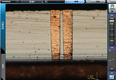
TSV technology (through-silicon via technology), commonly referred to as silicon via technology, is a new technical solution for interconnecting stacked chips in 3D integrated circuits, enabling the highest density of stacked chips in the 3D direction, the shortest interconnect lines between chips, the smallest form factor, and greatly improving chip speed and low-power performance. YW MEMS are equipped with the latest TSV technology and can meet customer individual TSV requirements. |
As one of the most promising technologies in microelectronics manufacturing, TSV technology is already widely used in MEMS devices, memories, image sensors, power amplifiers, bio-applications and various mobile phone chips. |
Opening size: 20-30um Depth to width ratio: 5:1 Electroplating material: Cu、Sn Through hole status: hollow hole |
Professionally provide chip design and research and development for enterprises
Full range of fabrication with good quality
1-to-1 foundry Service Checking all levels for clients
24-hour response Delivered as planned
Confidentiality agreements fabrication safety and security
Serving major universities and research institutes across the country to help scientific research
Online consultation
Project evaluation
Contract signing
Project implementation
Project delivery
After-sales service
 Links: Baidu
| Phone: 0512-67266051 | |
| E-mail: sales-mems@ywmems.com | |
Address:G202, No.338 Ruoshui Road, |

Copyrights YW MEMS © ICP 15018093-6 Su Gong An Bei NO.32059002002439 sitemap
